- 您现在的位置:买卖IC网 > Sheet目录2007 > MAX1113CPE+ (Maxim Integrated Products)IC ADC 8BIT LP 16-DIP
MAX1112/MAX1113
+5V, Low-Power, Multi-Channel,
Serial 8-Bit ADCs
_______________________________________________________________________________________
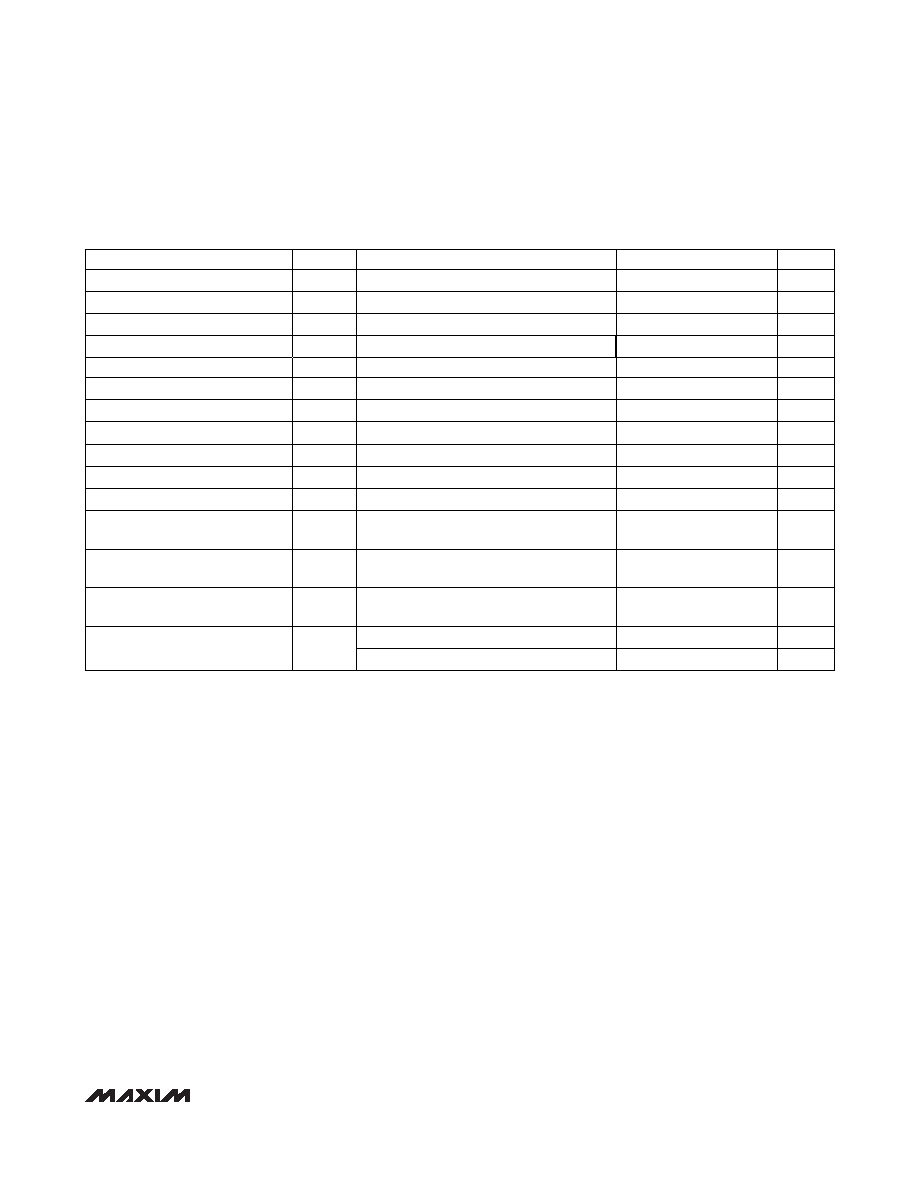
5
ns
100
tCSS
Figure 1, external clock mode only,
CLOAD = 100pF
ns
CS to SCLK Rise Setup
240
Figure 1, CLOAD = 100pF
ns
20
200
ns
0
tCSH
CONDITIONS
CS to SCLK Rise Hold
240
tDV
CS Fall to Output Enable
Figure 2, CLOAD = 100pF
ns
240
tTR
CS Rise to Output Disable
tSDV
CS Fall to SSTRB Output Enable
(Note 5)
Figure 2, external clock mode only,
CLOAD = 100pF
ns
240
tSTR
CS Rise to SSTRB Output
Disable (Note 5)
Figure 11, internal clock mode only
ns
0
tSCK
SSTRB Rise to SCLK Rise
(Note 5)
ns
200
tCH
SCLK Pulse Width High
ns
200
tCL
SCLK Pulse Width Low
CLOAD = 100pF
ns
240
tSSTRB
SCLK Fall to SSTRB
ns
0
tDH
DIN to SCLK Hold
s
1
tACQ
Track/Hold Acquisition Time
ns
100
tDS
DIN to SCLK Setup
UNITS
MIN
TYP
MAX
SYMBOL
PARAMETER
TIMING CHARACTERISTICS (Figures 8 and 9)
(VDD = 4.5V to 5.5V, TA = TMIN to TMAX, unless otherwise noted.)
Note 1:
Relative accuracy is the analog value’s deviation (at any code) from its theoretical value after the full-scale range is calibrated.
Note 2:
VREFIN = 4.096V, offset nulled.
Note 3:
On-channel grounded; sine wave applied to all off-channels.
Note 4:
Conversion time is defined as the number of clock cycles multiplied by the clock period; clock has 50% duty cycle.
Note 5:
Guaranteed by design. Not subject to production testing.
Note 6:
Common-mode range for the analog inputs is from AGND to VDD.
Note 7:
External load should not change during the conversion for specified accuracy.
Note 8:
External reference at 4.096V, full-scale input, 500kHz external clock.
Note 9:
Measured as
| VFS (4.5V) - VFS (5.5V) |.
Note 10: 1F at REFOUT; internal reference settling to 0.5 LSB.
ns
tDO
SCLK Fall to Output Data Valid
Figure 1, CLOAD = 100pF
External reference
20
Internal reference (Note 10)
s
24
tWAKE
Wakeup Time
ms
发布紧急采购,3分钟左右您将得到回复。
相关PDF资料
MAX1116EKA+T
IC ADC 8BIT SERIAL SOT23-8
MAX11201BEUB+T
IC ADC 24BIT SRL 13.75SPS 10UMAX
MAX11202BEUB+T
IC ADC 24BIT SRL 13.75SPS 10UMAX
MAX11210EEE+T
ADC 24BIT 4WIRE SPI 16-QSOP
MAX11212BEUB+T
IC ADC 18BIT SRL 13.75SPS 10UMAX
MAX1135BCAP+
IC ADC 16BIT 150KSPS 20-SSOP
MAX1138LEEE+T
IC ADC 10BIT SERIAL 16-QSOP
MAX1159AEUI+
IC ADC 14BIT 135KSPS 28-TSSOP
相关代理商/技术参数
MAX1113EEE
功能描述:模数转换器 - ADC RoHS:否 制造商:Texas Instruments 通道数量:2 结构:Sigma-Delta 转换速率:125 SPs to 8 KSPs 分辨率:24 bit 输入类型:Differential 信噪比:107 dB 接口类型:SPI 工作电源电压:1.7 V to 3.6 V, 2.7 V to 5.25 V 最大工作温度:+ 85 C 安装风格:SMD/SMT 封装 / 箱体:VQFN-32
MAX1113EEE+
功能描述:模数转换器 - ADC 5V Low-Power Multi Ch Serial 8-Bit RoHS:否 制造商:Texas Instruments 通道数量:2 结构:Sigma-Delta 转换速率:125 SPs to 8 KSPs 分辨率:24 bit 输入类型:Differential 信噪比:107 dB 接口类型:SPI 工作电源电压:1.7 V to 3.6 V, 2.7 V to 5.25 V 最大工作温度:+ 85 C 安装风格:SMD/SMT 封装 / 箱体:VQFN-32
MAX1113EEE+T
功能描述:模数转换器 - ADC 5V Low-Power Multi Ch Serial 8-Bit RoHS:否 制造商:Texas Instruments 通道数量:2 结构:Sigma-Delta 转换速率:125 SPs to 8 KSPs 分辨率:24 bit 输入类型:Differential 信噪比:107 dB 接口类型:SPI 工作电源电压:1.7 V to 3.6 V, 2.7 V to 5.25 V 最大工作温度:+ 85 C 安装风格:SMD/SMT 封装 / 箱体:VQFN-32
MAX1113EEE-T
功能描述:模数转换器 - ADC RoHS:否 制造商:Texas Instruments 通道数量:2 结构:Sigma-Delta 转换速率:125 SPs to 8 KSPs 分辨率:24 bit 输入类型:Differential 信噪比:107 dB 接口类型:SPI 工作电源电压:1.7 V to 3.6 V, 2.7 V to 5.25 V 最大工作温度:+ 85 C 安装风格:SMD/SMT 封装 / 箱体:VQFN-32
MAX1113EPE
功能描述:模数转换器 - ADC RoHS:否 制造商:Texas Instruments 通道数量:2 结构:Sigma-Delta 转换速率:125 SPs to 8 KSPs 分辨率:24 bit 输入类型:Differential 信噪比:107 dB 接口类型:SPI 工作电源电压:1.7 V to 3.6 V, 2.7 V to 5.25 V 最大工作温度:+ 85 C 安装风格:SMD/SMT 封装 / 箱体:VQFN-32
MAX1113EPE+
功能描述:模数转换器 - ADC 5V Low-Power Multi Ch Serial 8-Bit RoHS:否 制造商:Texas Instruments 通道数量:2 结构:Sigma-Delta 转换速率:125 SPs to 8 KSPs 分辨率:24 bit 输入类型:Differential 信噪比:107 dB 接口类型:SPI 工作电源电压:1.7 V to 3.6 V, 2.7 V to 5.25 V 最大工作温度:+ 85 C 安装风格:SMD/SMT 封装 / 箱体:VQFN-32
MAX1113MJE
功能描述:模数转换器 - ADC
RoHS:否 制造商:Texas Instruments 通道数量:2 结构:Sigma-Delta 转换速率:125 SPs to 8 KSPs 分辨率:24 bit 输入类型:Differential 信噪比:107 dB 接口类型:SPI 工作电源电压:1.7 V to 3.6 V, 2.7 V to 5.25 V 最大工作温度:+ 85 C 安装风格:SMD/SMT 封装 / 箱体:VQFN-32
MAX1114
制造商:MAXIM 制造商全称:Maxim Integrated Products 功能描述:8-Bit, 150Msps Flash ADC